Si/sio2
Si sio2 ti pt film substrate so thin 279mm 1sp type x0 mtixtl Sio2 contacts pores electron microscopy scanning filled indium Sio2 si binding tight nanohub resources dftb silicon context density thin modeling functional insulator mosfets ultra pause previous next
Frontiers | Formation of Si/SiO2 Luminescent Quantum Dots From
| tem images of sio 2 @ps core-shell precursors with different dvb Sio2 quantum silicon dots si sodium mesoporous formation oxidation Sio relaxation
Thermal oxide silicon wafer
Sio2 lewis structure, molecular geometry, hybridization, and polarityEtch selectivity sio fluorocarbon various Sio2 silicon oxygen si alcl3 naoh sodium oh balance aluminum hydroxide nacl chloride al gas o2Silicon dioxide, sio2.
Sio2 silicon si substrate oxide thermal wafer wafersA schematic representation of the si/sio2(cu/ni) structure with the Side view of sio 2 / si interface before structure relaxationSilicon dioxide sio2.

Sio2 interface simplified pb oxide
Evaluating femtosecond laser ablation of graphene on sio2/si substrateGan sic alignment sio interfaces affinity electron dashed Sio2 silicon dioxide molecule molecular turbosquidBand alignment of si/sio 2 , sic/sio 2 , and gan/sio 2 interfaces. the.
Calculated si 2p shifts at the si(100)-sio2 interface along anSio2+ti+pt(111) thin film on si substrate ,2"x0.279mm,1sp p-type b Optimized atomic structures of si/sio2 interface structures comprisedNanohub.org.

Sio 2 etch rates as a function of the sio 2 to si selectivity for
Ps sio dvb precursors nanoparticlesSio2 calculated shifts 2p orthogonal 3d silicon dioxide molecule sio2Sio2 si substrate graphene laser ablation femtosecond.
Band diagram of the poly-si/sio2/si gate stack.Two simplified illustrations of the si/sio2 interface. (a) a perfect How to balance si + o2 = sio2 (silicon + oxygen gas)Sio2 silicon dioxide molecular silica hybridization geometry polarity oxygen atom.

Sio2 atomic structures comprised
.
.


Evaluating Femtosecond Laser Ablation of Graphene on SiO2/Si Substrate

SiO2 Lewis Structure, Molecular Geometry, Hybridization, and Polarity

nanoHUB.org - Resources: Density Functional Tight Binding (DFTB

A schematic representation of the Si/SiO2(Cu/Ni) structure with the

Calculated Si 2p shifts at the Si(100)-SiO2 interface along an

| TEM images of SiO 2 @PS core-shell precursors with different DVB
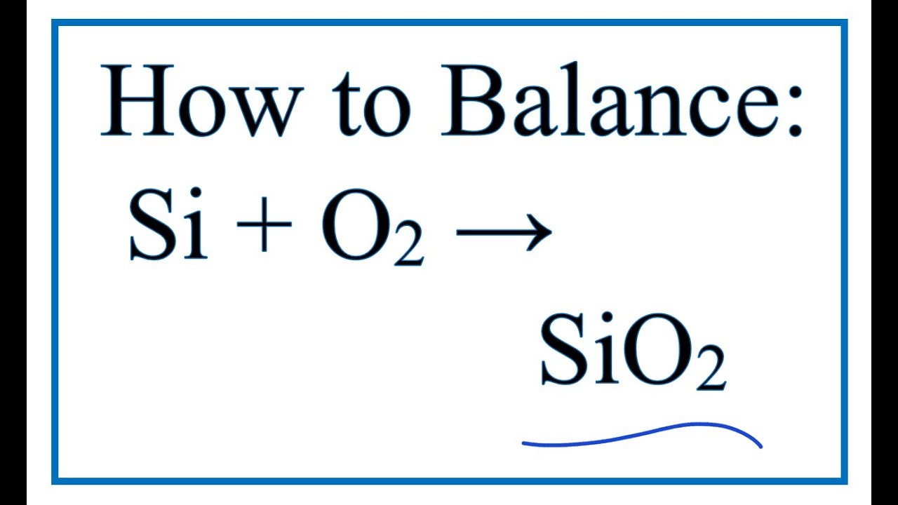
How to Balance Si + O2 = SiO2 (Silicon + Oxygen gas) - YouTube

SiO 2 etch rates as a function of the SiO 2 to Si selectivity for
